

赫狄通納米
主營產(chǎn)品: 納米材料
基于鎳箔的CVD石墨烯薄膜(4英寸晶圓)
價(jià)格
訂貨量(件)
¥4650.00
≥1
店鋪主推品 熱銷潛力款
잵잰잱잵잴잳잲잴잲잰재
在線客服
生產(chǎn)廠商:Graphene Supermarket
產(chǎn)品信息
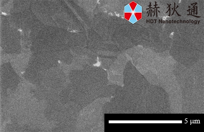
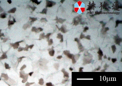
Graphene on nickel is a few monolayers thick, usually between 1-7 layers with an average of 4 monolayer thickness. It looks like a patchwork, whereas each “patch” has a different thickness. The graphene layers within the same patch are aligned relative to each other (there is a graphitic AB-stacking order). The size of each patch is about 3-10 microns.
Because graphene on nickel is grown in patches with different layering, the Raman signal will change dramatically depending on the spot of the film where it is taken. If nickel is used as a catalyst, it is not possible to create a graphene sheet with a precise and uniform layering.
? Graphene Electronics
? Conductive Coatings
? Aerospace Industry
? Support for Metallic Catalysts
? Microactuators
? MEMS and NEMS
? Chemical and Bio Sensors
? Multifunctional Materials Based on Graphene
? Graphene Research


采購數(shù)量不能為空
聯(lián)系信息不能為空

驗(yàn)證碼不正確